|
 |
|
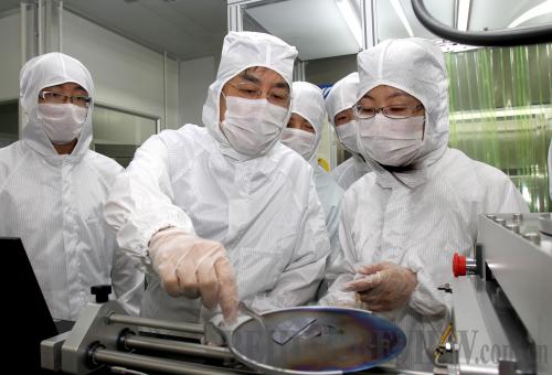
TEAM SPIRIT: Wang Xi (second left) conducts an experiment on SOI technology with his colleagues in a lab at the Shanghai Institute of Microsystem and Information Technology on August 26 (LIU YING) |
At the age of 43, Wang Xi became the youngest academician with the Chinese Academy of Sciences (CAS) in 2009. Wang is known in academic circles as a talented and modest scientist who has made outstanding achievements in the field of semiconductor research and development. In 2008, he developed China's first 8-inch bonding silicon-on-insulator (SOI) wafer, a significant breakthrough in SOI wafer technology. This year, Wang was selected as a delegate to the 18th National Congress of the Communist Party of China.
SOI is a cutting-edge technology in the field of micro-electronics and photoelectron spectroscopy for developing next generation silica-based material and new integrated circuits used in the electronics industry. For instance, computers are getting much smaller with higher processing power and lower energy consumption while smart cell phones have become widely used. And ion injection—the key to making SOI—is what Wang has researched for years.
Wang was born in Shanghai in 1966. He graduated from Tsinghua University in 1987 and went on to earn a Ph.D. in materials physics in CAS' Shanghai Institute of Metallurgy in 1993, which was renamed the Shanghai Institute of Microsystem and Information Technology (SIMIT) in 2001.
After graduation, Wang worked as a researcher in SIMIT and later dedicated himself to researching the interaction between energetic particle beams and solids, with research interests covering advanced electronic materials and functional thin-layer materials.
In 1996, his excellent performance earned Wang entry into Germany's Forschungszentrum Rossendorf for visiting research as a Humboldt Fellow. He had the option of staying in Germany permanently to study ion injection. "The days in Germany were very comfortable. I was satisfied with the pleasant residence and advanced scientific research facilities. But I had to make a choice between returning to my home country and staying overseas," Wang said to Beijing Review. "I was irresolute for a while."
At the same time, the director of SIMIT, who was also Wang's superior, went to Germany. The two of them took a walk along the banks of the Rhine River. "The director told me that CAS was carrying out a major science program that offered many favorable polices for returning scientists. He hoped that I could seize the opportunity to pursue a breakthrough in my career and make a contribution to the country," Wang recalled.
Wang declined the invitation from the German science institute and returned to China with his wife and their new-born child in 1998. "When looking back today, returning to China was the most important and right decision in my life," Wang said. "Only with the support of his country can a scientist conduct scientific inquiries independently and realize his ambition."
That year, the computer giant IBM announced efforts to apply SOI materials into the development of digital products, leading to mass production of large-scale computer servers and chips. A large number of international corporations soon rushed into the field of this cutting-edge technology. In the early 1980s, China's SOI technology was limited to the field of aerospace and defense. "For over 10 years, SOI appeared in China only in academic papers and theories. We did not have adequate equipment and technology to make consumer SOI products. We were far behind the international scientific frontier," Wang recalled.
Faced with the urgent task, Wang immediately accepted the appointment as head of the Ion Beam Development & Research Lab of CAS as soon as he returned to Shanghai at the age of 32. His job was to lead an elite team to work on a number of national-level projects, including the key project of ULSI Auxiliary Materials in the national 863 Plan. He hoped to make a breakthrough in SOI research and development. "I thought about nothing but the research all day," Wang said.
Wang's ambitious team started from scratch, working overtime in the lab on a routine basis. Wang did everything in person, from purchasing machines and equipment to making SOI wafers. The experiments were not immediately successful due to the team's inexperience. The wafers made in those early days had many flaws, requiring immense effort to perfect the process.
|